PCB Assembly Service
-
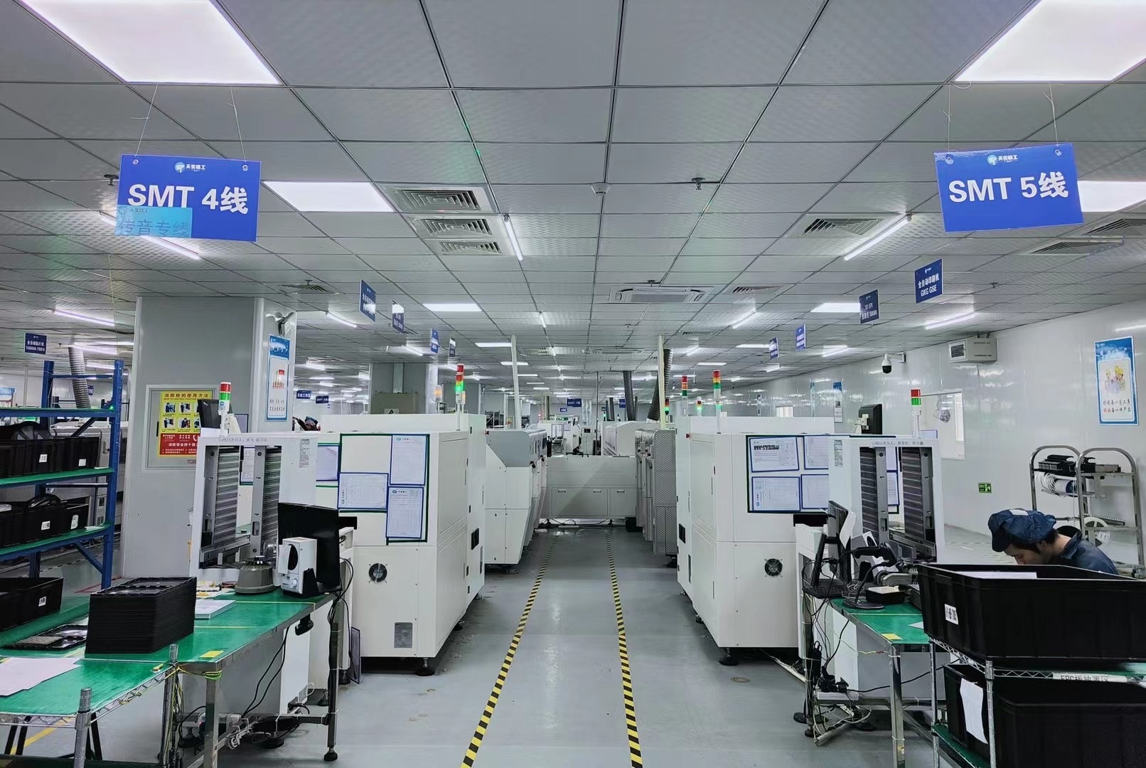
SMT ASSEMBLY
Our SMT assembly team is composed of certified technicians who possess extensive experience in delivering top-notch electronic manufacturing services.
-
THROUGH-HOLE ASSEMBLY
Our through-hole assembly team comprises highly skilled technicians with extensive experience in providing electronic manufacturing services.
-
LEAD-FREE PACKAGES
Lead-freepackages are widely used in the production of small electronic devices, and we have extensive experience in handling them.
Capabilities Of PCB Assembly
| Item | Capacity | Item | Capacity | ||
| 1 | Single and double sided SMT/PTH | Yes | 13 | PCB Finish | SMOBC/HASL Lead free |
| 2 | Single and double sided SMT/PTH | Yes | Electrolytic gold | ||
| 3 | Smallest Chips size | 0201 | Electroless gold | ||
| 4 | Min BGA and Micro BGA pitch and ball counts | 0.008 in. (0.2mm) pitch, ball count greater than 1000 | Electroless silver | ||
| 5 | Min Leaded parts pitch | 0.008 in. (0.2 mm) | Immersion gold | ||
| 6 | Max Parts size assembly by machine | 2.2 in. x 2.2 in. x 0.6 in. | Immersion tin | ||
| 7 | Assembly surface mount connectors | Yes | OSP | ||
| 8 | Assembly surface mount connectors | Yes | 14 | PCB Shape | Any |
| LED | 15 | Panelized PCB | Tab routed | ||
| Resistor and capacitor networks | Breakaway tabs | ||||
| Electrolytic capacitors | V-Scored | ||||
| Variable resistors and capacitors (pots) | Routed+ V scored | ||||
| Sockets | 16 | Inspection | X-ray analysis/Microscope to 20X/AOI | ||
| 9 | Wave soldering | Yes | FCT/ICT | ||
| 10 | Max PCB size | 14.5 in. x 19.5 in. | 17 | Rework | BGA removal and replacement station |
| 11 | Min PCB Thickness | 0.004 in. | SMT IR rework station | ||
| 12 | Fiducial Marks | Preferred | Thru-hole rework station |
PCB Assembly Manufacturing Process
PCBA stands for "Printed Circuit Board Assembly." It is a crucial step in the manufacturing of electronic devices. PCBA involves assembling various electronic components onto a printed circuit board (PCB) to create a functional electronic circuit. Here's an overview of the PCBA process:
Design
The process begins with the design of the PCB. Electronic engineers and designers use specialized software to create a PCB layout that specifies the placement of components and the interconnections between them. This design is then used to create the actual PCB.
PCB Fabrication
The PCB design is sent to a fabrication facility, where the PCB is manufactured. This involves the etching of copper layers, drilling holes, and applying various coatings to create the finished PCB.
Component Procurement
Once the PCBs are ready, the next step is to source the electronic components required for the assembly. These components may include resistors, capacitors, integrated circuits (ICs), connectors, and more. They are typically purchased from component suppliers.
Stencil Creation
A stencil is used to apply solder paste to the PCB. This paste will act as an adhesive for the components. The stencil is typically made of stainless steel and is custom-designed to match the PCB layout.
Solder Paste Application
Solder paste is applied to the PCB through the stencil, typically using a screen printing process. This paste is applied to the pads where the components will be placed.
Component Placement
Based on the packaging specifications of these components, there are primarily two assembly methods: SMT (Surface Mount Technology) is mainly used for components with soldering pads suitable for surface mounting, while DIP (Dual In-line Package) assembly is mainly employed for components with soldering pins designed for through-hole mounting.
Typically, PCB component assembly begins with SMT, which is often automated through machine equipment and programmed instructions. DIP assembly, on the other hand, is typically manual labor-intensive, although there are automated DIP assembly machines available. However, it's important to note that DIP assembly equipment is generally more expensive than SMT assembly machines.
Currently, the majority of electronic components on PCBs have transitioned from older through-hole assembly to predominantly SMT assembly, with only a few through-hole components, or even none at all.
Therefore, unless a particular PCB requires a significant number of through-hole components and is produced in large quantities, manual assembly is the common practice.
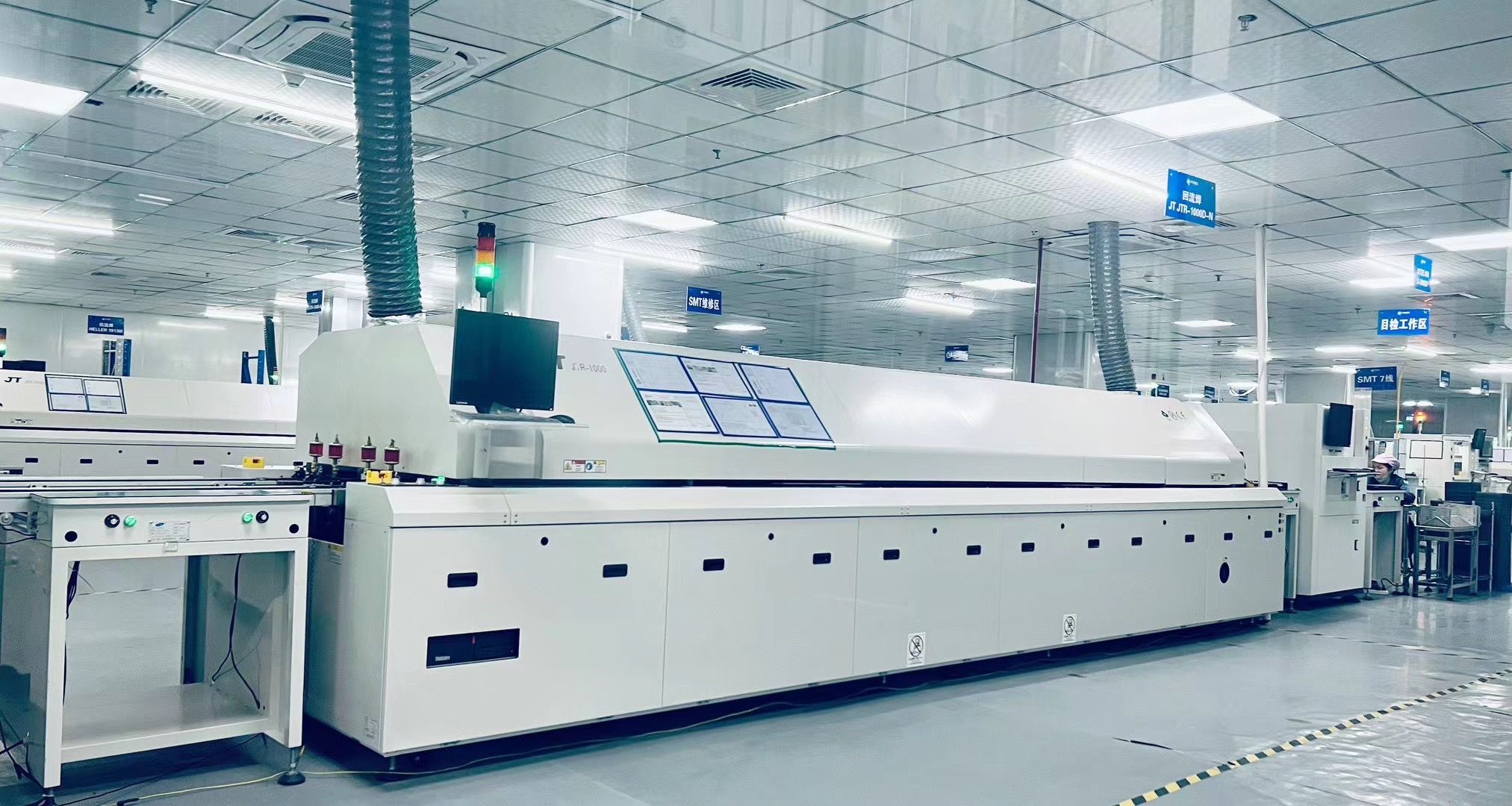
Reflow Soldering
The assembled PCB is then passed through a reflow oven. In the oven, the solder paste is heated, causing it to melt and create a permanent connection between the components and the PCB. This process ensures that the components are securely attached to the PCB.
Inspection
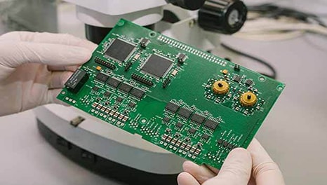
After reflow soldering, the PCBAs go through a series of inspections. Automated optical inspection (AOI) and other techniques are used to check for defects, such as missing components or incorrectly placed components, reverse, poor soldering or components damage. Any defects are typically flagged for rework.
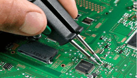
Rework
If defects are found, the PCBAs may undergo rework, where faulty components are replaced or solder joints are corrected.
Testing
Once the assembly is deemed defect-free, it goes through functional testing to ensure that it operates as intended. This may include testing for electrical continuity, functionality, and performance.
Cleaning
Some PCBAs undergo a cleaning process to remove any residues left from the soldering process. This step is particularly important for PCBAs that require a high degree of cleanliness, such as those used in medical devices or aerospace applications.
Packaging and Shipping
After successful testing and cleaning, the PCBAs are packaged and prepared for shipment to the manufacturer's customers, where they will be incorporated into the final electronic products.
The PCBA process is a critical step in electronics manufacturing and requires precision and quality control to ensure the reliability and functionality of electronic devices. Automated machinery is often used to increase efficiency and consistency in the assembly process.
-
Q What is your MOQ(Minimum Order Quantity)?


We have no MOQ limited.Sample and mass production all can support.
-
Q What is needed for quotation?
FPC&rigid-flex PCB&PCB:Quantity, Gerber file and Technical requirements(material,surface finish treatment, copper thickness,board thickness ,...)
PCBA:PCB information, BOM list -
Q Can you manufacture my PCB from a picture?
No, we cannot accept BMP, GIF, TIFF, or JPG pictures as the manufacturing file.If you do not have gerber file, you can send us sample to copy it.
-
Q Are my files safe?
We ensure complete safety and security of your files and protect our customers' intellectual property throughout the entire process. Any documents provided by our customers are kept strictly confidential and are never shared with any third parties.
-
Q How long will it take to receive my quotation?
We will respond your quotation within 24 hours to the quotation requests.
-
Q How can I pay?
We accept payments by PayPal, cash, bank transfer (T/T),WU,Alipay. If need other payment method please contact us (sienta@sienta.com.cn).
-
Q What's your transport method?
We use UPS, FedEx, or DHL to ship the boards. If you have your own freight forwarding company, we can also work with them.
-
Q Do you offer free sample?
We can offer samples, but you must pay for them first. If you go ahead with mass production later on, the cost of the samples will be deducted.We look forward to establishing a long-term business relationship with you!
-
Q What is your standard lead time?
As FPC&PCB belong to customized products,generally it is 3-7 days for samples and 10-20 days for mass products.The actual delivery date according to difficulty of the products, the quantity and etc.Please contact us to get different product lead time.
-
Q How do you control the product quality?
We adhere to strict quality control standards set by ISO 9001, ISO 14001, IATF 16949, and SGS. All boards undergo 100% testing and we offer a range of inspection options including visual, X-ray, AOI, and ICT/FCT.
-
Q How many layer can you produce for flexible PCB?
For FPC, we can produce from 1 layer to 8 layers.
-
Q How many layer can you produce for Rigid flexible PCB?
For Rigid flexible PCB board, we can produce from 2 layer to 8 layers.
-
Q Which surface treatment can you produce for FPC, PCB and rigid flexi PCB?
We can produce Immersion gold, immersion silver, OSP, hot air Levelling(L/F), Gold plating,ENIPIG, Immersion tin and etc.