PCBA is a crucial step in the manufacturing of electronic devices. It involves the assembly of electronic components onto a printed circuit board, creating a functional and interconnected system. In this article, we will delve into the PCBA manufacturing process, highlighting the key stages from design to assembly.
The first stage of the PCBA manufacturing process is the design phase. During this stage, engineers work closely with the product development team to design the circuit board layout, taking into account the functionality, size, and electrical requirements of the device. Design software, such as CAD (Computer-Aided Design), is used to create a digital representation of the circuit board.
Once the design is finalized, the next step is component procurement. This involves sourcing and purchasing the electronic components required for the assembly. Components can be sourced from various suppliers, and factors like cost, availability, and quality are considered during the selection process. It is crucial to ensure that the components are genuine and meet the required specifications.
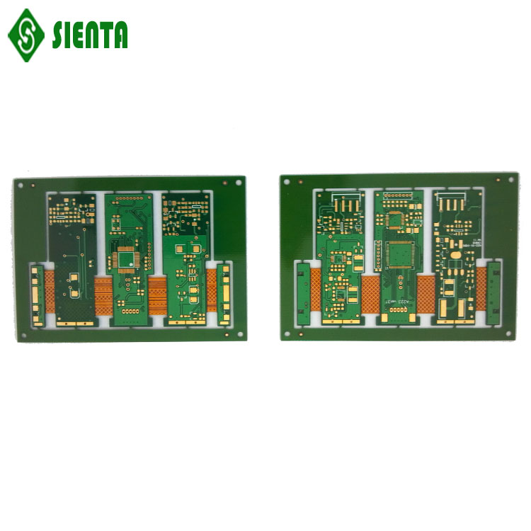
With the components ready, the focus shifts to manufacturing the printed circuit board (PCB). The PCB is the foundation on which the components will be mounted. The manufacturing process involves several steps, including etching, drilling, and copper plating. Advanced techniques like surface mount technology (SMT) and through-hole technology (THT) are used to create the necessary connections and pads on the board.
Once the PCB is ready, the next stage is component placement. This involves the precise positioning of the electronic components onto the board. Automated machines, known as pick-and-place machines, are used for this purpose. These machines can handle a wide range of component sizes and accurately place them onto the designated locations on the board. The components are held in place temporarily using solder paste.
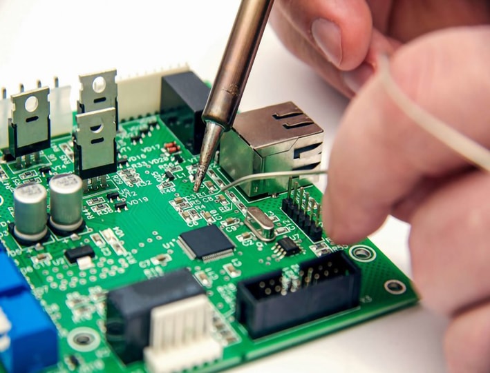
After component placement, the PCB goes through the soldering process. There are two primary methods of soldering: reflow soldering and wave soldering. In reflow soldering, the PCB is heated in a controlled manner to melt the solder paste, creating permanent connections between the components and the board. Wave soldering, on the other hand, involves passing the PCB over a wave of molten solder, which solders the components from beneath.
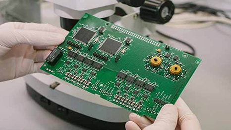
Once the soldering process is complete, the assembled PCB undergoes thorough inspection and testing. Automated optical inspection (AOI) machines are used to detect any defects, such as misaligned components or soldering issues. Functional testing is also performed to ensure that the assembled PCB operates as intended. Any faulty components or solder joints are identified and rectified at this stage.
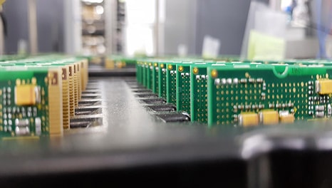
The final stage of the PCBA manufacturing process involves packaging and delivery. The assembled PCBs are carefully packaged to protect them during transportation. Documentation, including test reports and certificates of conformity, may also be included. The packaged PCBs are then shipped to the customer or the next stage of the production line.
The PCBA manufacturing process is a complex and intricate procedure that requires careful planning, precise execution, and stringent quality control measures. From the initial design phase to the final packaging and delivery, each step plays a crucial role in ensuring the production of high-quality electronic devices. By understanding the various stages involved in PCBA manufacturing, we gain insight into the intricate process behind the electronic devices we use in our daily lives.

Sienta Industry is a professional factory specializing in the production of FPC,PCB assembly, Rigid-Flex PCB with fast delivery and high quality.
By continuing to use the site you agree to our privacy policy Terms and Conditions.