Drilling

Three common types of drilling holes in PCB:VIA holes, blind holes, and buried holes

Let's first introduce the meaning and characteristics of these three types of holes in PCB: VIA holes, blind holes, and buried holes.
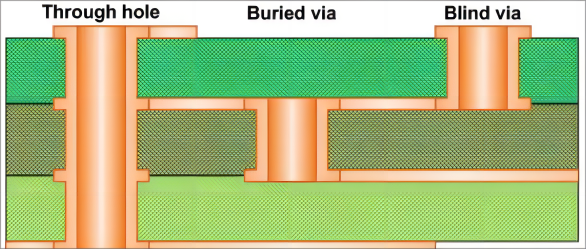
VIA Holes

Definition:

This is a common hole is used to conduct or connect the copper foil lines between the conductive graphics in different layers of the board with. For example (such as blind holes, buried holes), but can not be inserted into the assembly lead leg or other reinforcing material copper-plated holes. Because the PCB is formed by the accumulation of many layers of copper foil stacked, each layer of copper foil will be laid between a layer of insulation, so that the copper foil layers can not interoperate with each other, the link between the signals on the conductive holes (via).

Features:

In order to meet different demands, the board's conducive hole must be plugged, so that in changing the traditional aluminum plug hole process, with a white network to complete the board surface blocking and plug holes, so that its production is stable, reliable quality, the use of more perfect. VIA hole is mainly to play the role of circuit interconnection conduction, with the rapid development of the electronics industry, but also on the printed circuit board production process and surface mount technology has put forward higher requirements.VIA hole for plugging hole process is applied and born, at the same time should meet the following requirements:

·VIA hole can have copper, solder can be plugged or not.

·VIA hole must have tin lead, there is a certain thickness requirements (4um) shall not have solder resist ink into the hole, resulting in the hole has hidden tin beads.

·VIA hole must have solder resist ink plugging hole, not transparent, shall not have tin ring, tin beads and flat and other requirements.

Blind Hole

Definition:

It is the outermost circuit in the PCB and the adjacent inner layer to connect with plated holes, because we can not see the opposite side, so called blind pass. At the same time to increase the use of space between PCB circuit layers, blind holes are applied. That is, to a surface of the printed circuit board of the conductive holes.

Features:

Blind holes are located on the top and bottom surface of the board, with a certain depth, for the link between the surface lines and the inner layers below, the depth of the hole usually does not exceed a certain ratio (hole diameter). This production method requires special attention to the depth of the hole (Z axis) to be just right, do not pay attention to the hole will cause plating difficulties, so almost no factory to use, but also the need to connect the circuit layer in advance of the individual circuit layer when the hole is first drilled, and then finally glued together, but requires more sophisticated positioning and alignment devices.

Buried Holes

Definition:

PCB internal link between any circuit layers but not conductive to the outer layer, is also not extended to the surface of the board conductive hole means.

Features:

In this process can not be used after the bonding of the drilling method to achieve, must be in the individual circuit layer when the implementation of drilling, first partial bonding of the inner layer after the first plating treatment, and finally to all bonding, than the original lead-through holes and blind holes to more work, so the price is also the most expensive. This process is usually used only for high-density boards to increase the available space for other circuit layers.

In the PCB production process, drilling is very important and should not be sloppy. This is because drilling is the process of drilling the required holes in the laminate to provide electrical connections and hold the devices in place. If the operation is not proper, the process of over-hole problems, the device can not be fixed on top of the board, the light affect the use of the whole board will be scrapped, so the drilling process is quite important.

Leave a Message

Get a fast FPC or PCBA quote from the experts

Upload attachments
captcha
×

Contact Us

captcha
×

Inquire

*Name
*Email
Company Name
Tel
*Message