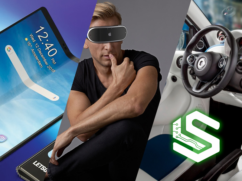
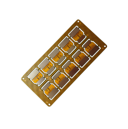
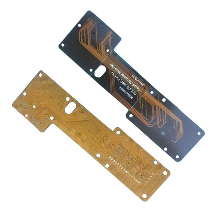
Flexible Printed Circuits (
FPCs) are widely used in smartphones, wearable devices, automotive electronics, and more due to their thin, lightweight, bendable, and highly integrated characteristics. The manufacturing process combines precision material science with complex process control. Below is a detailed breakdown of the full FPC production process:

1. Material Preparation: Substrate and Copper Foil Selection
Substrate (PI/PET Films)
Polyimide (PI) film is the mainstream choice, offering high-temperature resistance (withstands 400°C+ during short-term soldering) and excellent bendability (dynamic bending life > 100,000 cycles).
Thickness range: 12.5μm~125μm, with a tolerance of ±5%.
Copper Foil Treatment
Electrodeposited Copper (ED): Lower cost but higher roughness (Rz > 3μm), suitable for general applications.
Rolled Annealed Copper (RA): Better ductility (>20%) and smoother surface (Rz < 1.5μm), ideal for high-frequency/dynamic bending applications.
Coverlay
Made of PI or PET film with epoxy adhesive, thickness 50μm~100μm, used to protect circuits and provide insulation.
2. Pattern Transfer: Photolithography Process
Photoresist Coating
Dry film or liquid photoimageable (LPI) process, thickness 5μm~15μm.
Dry film is laminated using heat and pressure (80~100°C, 0.3~0.5MPa).
Exposure and Development
UV exposure (wavelength 365nm, energy 100~300mJ/cm²), followed by development (1% sodium carbonate solution) to remove uncured resist.
Line width precision: ±10μm (high-end products require ±5μm).
3. Etching: Precision Copper Circuit Formation
Chemical Etching
Etching solution: Ferric chloride (FeCl₃) or alkaline copper chloride (ammonia + copper chloride), temperature 40~50°C.
Undercut control: Spray pressure (0.2~0.4MPa) minimizes undercut, line width deviation < ±8%.
Stripping and Cleaning
Stripping solution (3%~5% sodium hydroxide) removes photoresist, followed by plasma cleaning (Ar/O₂) to eliminate residues.
4. Lamination: Precision Bonding of Multilayer Structures
Lamination Process
Coverlay and substrate are pre-bonded using a vacuum laminator (temperature 170~190°C, pressure 0.8~1.2MPa).
Key metrics: No bubbles (visual inspection), bonding accuracy ±25μm.
Stiffener Design
Local reinforcement with FR4/PI stiffeners (thickness 0.1~0.3mm), bonded using thermosetting adhesive (epoxy resin) to enhance connector area strength.
5. Drilling and Plating: Creation of Vias
Laser Drilling
CO₂ laser (wavelength 9.4μm) or UV laser (wavelength 355nm), hole diameter 50~150μm, precision ±10μm.
High-speed drilling: 5000~10,000 holes/minute (for high-density HDI boards).
Electroless Copper Deposition (PTH)
Hole wall activation → Electroless copper deposition (thickness 0.3~1μm) → Electroplating (copper thickness 15~25μm).
Conduction resistance requirement: <50mΩ (test voltage 1V).
6. Surface Finish: Protection and Solderability Enhancement
Flash gold: Higher abrasion resistance, good electrical conductivity and stability.
Electroless Nickel Immersion Gold (ENIG): Nickel layer 3~5μm, gold layer 0.05~0.1μm, suitable for high-frequency signals.
OSP (Organic Solderability Preservative): Low cost but short shelf life (<6 months).
7. Testing and Reliability Verification
Electrical Testing
Flying probe testing (100% coverage) or fixture testing, impedance control (TDR test tolerance ±7%).
Environmental Testing
Dynamic bending test (IPC-6013 standard): Bend radius 5mm, >100,000 cycles without failure.
High-temperature/humidity test (85°C/85%RH, 1000 hours), impedance change <10%.
8. Applications and Emerging Trends
Typical Applications
Foldable Smartphones: Bend radius <3mm, dynamic life >200,000 cycles.
Automotive Radar: High-frequency (77GHz) impedance matching (±5Ω), using ultra-low roughness copper foil.
Technology Trends
Roll-to-Roll (R2R) Process: Improves mass production efficiency, reduces costs by 30%.
Embedded Components: Integrating resistors/capacitors within FPCs to reduce size.
Conclusion: Core Challenges in FPC Manufacturing
Precision: Line width/spacing <50μm requires nanometer-level etching control.
Reliability: Stability under harsh conditions like dynamic bending and high-temperature/humidity environments.
Cost: Materials account for >60% of costs, necessitating a balance between performance and production economics.
Through precision processes and intelligent control (e.g., AI defect detection), FPCs are driving continuous innovation in consumer electronics, medical devices, and beyond.
As a dual-certified FPC manufacturer with both IATF 16949 and ISO 14001, we provide one-stop solutions from prototyping to mass production. Whether it is consumer electronics, automotive electronics or medical devices, Sienta can provide you with the best quality FPC products.