News
Site Editor
 Site
/uploads/image/667d0e0257f45.png
During the design process of FPCs (Flexible Printed Circuits), although many aspects are similar to those of PCB (Printed Circuit Board) design, such as drilling, board outline, circuitry, solder mask, and legend design, FPCs require special attention to certain critical details due to their flexible nature. The following are some key guidelines to avoid potential issues:
Site
/uploads/image/667d0e0257f45.png
During the design process of FPCs (Flexible Printed Circuits), although many aspects are similar to those of PCB (Printed Circuit Board) design, such as drilling, board outline, circuitry, solder mask, and legend design, FPCs require special attention to certain critical details due to their flexible nature. The following are some key guidelines to avoid potential issues:
How to avoid FPC design pitfalls
Views: 1934
Author: Site Editor
Publish Time: 2025-01-03
Origin: Site
During the design process of
FPCs (Flexible Printed Circuits), although many aspects are similar to those of PCB (Printed Circuit Board) design, such as drilling, board outline, circuitry, solder mask, and legend design, FPCs require special attention to certain critical details due to their flexible nature. The following are some key guidelines to avoid potential issues:

I. Outline and Drilling Design
1.Ensure a minimum distance of 0.5mm between the hole edge and the outline. If less than this value, consider a U-shaped hole design to avoid potential problems associated with direct connection between the hole and outline edges.
2.Maintain a distance of at least 0.2mm between the via and the solder mask opening to prevent copper exposure around the hole, which could affect the performance and appearance of the circuit board.
3.Due to the inability of FPCs to perform resin plugging, designing buried vias may lead to risks of solder leakage, and is therefore not recommended.
II. Circuitry Design
1.It is advisable to convert large copper areas into grid designs to reduce oxidation issues caused by air entrapment during laminate pressing. Additionally, solder mask openings can be added to large copper areas to enhance the stability of the circuit board.
2.Avoid designing isolated pads as the thin base material of FPCs makes them prone to detachment. Instead, increase copper cladding and add connecting lines at the four corners of the pad, connecting them to the copper cladding. Moreover, the pads on both sides should be staggered to reduce stress concentration.
3.Minimize the design of large exposed copper areas to prevent wrinkling and oxidation.
4.Ensure a solder mask bridge of at least 0.5mm; otherwise, consider a full opening design.
5.Incorporate anti-tear copper strips at corners or add network copper on the backside to reduce the risk of tearing.
6.Recommend using a 45-degree angle for circuit grid design to improve signal transmission performance. Additionally, line width and spacing are suggested to be 0.2/0.2mm.

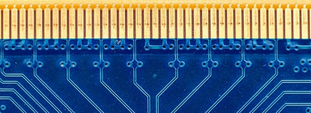
III. Gold Finger Design
1.Internally recess the gold fingers by 0.2mm to avoid micro-shorts caused by high-temperature carbonization during laser cutting.
2.Avoid arranging vias in a row on the pads of solderable fingers to reduce the risk of fracture due to stress concentration. Additionally, the upper and lower coverlays should be staggered by at least 0.3mm to prevent breaking.
3.The solder mask opening for gold fingers should overlap the pad by at least 0.3mm to prevent disconnection between the gold finger pad and its connection.
4.IC pads should avoid excess copper cladding to prevent pad enlargement and reduced spacing, which could lead to welding shorts. Gold finger pads should be designed as isolated pads to avoid copper or wire exposure after solder mask opening.
IV. Solder Mask Design
1.To prevent copper fracture in vias during bending, they are generally designed with solder mask coverage.
2.For double-sided boards with large exposed copper areas on the edges, consider adding a layer of coverlay around the edges to prevent darkening issues.
V. Panelization Design
1.The spacing between stiffener boards (using steel sheets) should be at least 3mm, with a slot width of 0.5mm and a connection point width of 1mm. Add connection points every 15mm or so.
2.Avoid placing panelization connection points on gold fingers to prevent unevenness at the front end.
3.Each piece should have at least 2 connection points, with a width of 0.8mm, depending on the board size. Smaller boards with too many connection points may make it difficult to separate them. If SMT is not required, each piece only needs 2 connection points of 0.3mm for easy manual separation.
4.Low panelization utilization can lead to higher quoting. Try to keep the panelization width at 119mm or 240/250mm, or allow the manufacturer to panelize as needed.
VI. Stiffener Design
1.PI stiffener is suitable for gold finger plugging products; FR4 is suitable for lower-end products; steel sheets provide good flatness and do not deform, making them suitable for products requiring chip mounting.
2.Avoid placing stiffener over component holes or pads to prevent shorts. Additionally, the stiffener height for gold fingers should be at least 1.0mm longer than the gold finger pad to prevent fracture during use.
By following these guidelines, you can improve the reliability and stability of your FPC designs, reducing potential production issues and costs.