Electronic manufacturing has evolved into a cornerstone of global industry, influencing applications ranging from consumer electronics to industrial equipment. Its growing importance is evident in its widespread applicability, playing a crucial role in modern society. Within electronic manufacturing, the assembly of 12-layer PCBs stands out as a defining process, representing the creation of intricate circuit boards with increased integration and enhanced performance capabilities. The augmentation of layers in 12-layer PCB assembly allows for greater layout space, accommodating a higher number of electronic components and propelling continuous technological innovation across various industries.
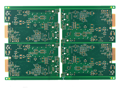
The significance of PCB layering lies in providing more layout space for increased integration, reduced electromagnetic interference, enhanced signal integrity, and simplified wiring complexity. Layering also lowers the overall complexity of the PCB, making it easier to design, manufacture, and maintain. The 12-layer PCB, with its 12 independent copper foil layers, offers a structural design that accommodates more electronic components and intricate circuit designs in a smaller space. Its inner and outer layers interconnected through vias create a complex structure ideal for high-performance electronic devices, meeting the demands of applications requiring high-density layouts and extensive connectivity.
The assembly of a 12-layer PCB provides significant advantages, including enhanced circuit density and complexity. This configuration allows for the accommodation of a greater number of electronic components and intricate circuit designs in a relatively small space. Improved signal integrity, achieved by reducing the length of signal transmission lines, makes it suitable for applications demanding high signal quality, such as communication devices and high-performance computers. The 12-layer PCB design also offers greater flexibility in arranging different functional modules across various layers, making it suitable for diverse and complex electronic applications.
Designing a 12-layer PCB presents challenges such as increased manufacturing complexity and costs. Balancing performance aspirations with cost-effectiveness becomes crucial. The intricate signal transmission paths in multi-layer designs pose challenges to signal integrity and impedance matching, requiring meticulous layout strategies. Higher power consumption and heat generation necessitate effective thermal management to prevent overheating and safeguard component integrity. Striking a harmonious equilibrium between performance optimization, manufacturing feasibility, signal integrity, and thermal considerations is vital for delivering a 12-layer PCB solution that meets stringent standards and functional requirements.
The assembly process involves selecting key materials, including substrate materials, copper thickness and types, and dielectric materials. Substrate materials, like FR-4, provide support and insulation, while the copper foil in the conductive layer plays a vital role in circuit conduction, requiring careful selection of appropriate thickness and types. Dielectric materials, such as FR-4 and high-frequency dielectrics, isolate different conductive layers, influencing signal transmission stability. The meticulous combination and selection of these material categories ensure the successful assembly of a 12-layer PCB, providing reliability and high performance.
The assembly process encompasses steps from circuit design to surface treatment, ensuring high quality and outstanding performance. It starts with design and drafting, followed by drilling, electroplating, printing identification marks, separation, and shaping processes. Surface treatment enhances corrosion resistance and durability. The synergy of Surface Mount Technology (SMT) and through-hole technology ensures the reliability and performance of the 12-layer PCB. SMT facilitates high-density circuit layouts through surface-adhered components, while through-hole technology provides additional mechanical support.
The widespread application of 12-layer PCB technology has brought innovation to various industries. In the medical sector, it has propelled the development of portable medical devices like monitors and imaging equipment, enhancing accuracy and meeting diverse application needs. In telecommunications, 12-layer PCB technology has driven innovation in communication devices and network base stations, supporting faster and more reliable data transmission. Successful case studies underscore the robust support provided by 12-layer PCB technology in improving equipment performance and meeting technological demands.
Anticipated trends include advancements driven by emerging technologies such as AI, IoT, and 5G communication, fostering the need for enhanced circuit board performance. Improvements in manufacturing processes, efficiency, and environmentally friendly production methods are expected. Precision in assembly processes will elevate the efficiency and quality of 12-layer PCB production. Potential applications of emerging technologies like flexible electronics and three-dimensional integration may broaden the scope of 12-layer PCBs, increasing their relevance across diverse sectors.
The rise of 12-layer PCB technology showcases its importance in electronic manufacturing, providing exceptional performance and flexibility. Continuous technological advancements in 12-layer PCBs play a crucial role in meeting the demands for high performance, density, and reliability in modern electronic products. Their widespread applications in healthcare and communication underscore their growing significance, contributing significantly to the evolution of electronic manufacturing and aligning with the ever-increasing requirements of modern electronic devices.

Sienta Industry is a professional factory specializing in the production of FPC,PCB assembly, Rigid-Flex PCB with fast delivery and high quality.
By continuing to use the site you agree to our privacy policy Terms and Conditions.