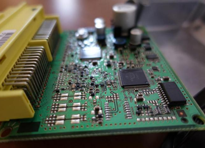
Two-layer PCBs, consisting of two substrate layers connected by an electrically conductive layer through vias, are commonly utilized in relatively simple electronic devices due to their straightforward structure and cost-effectiveness. Electrical connections on these boards primarily occur through copper foil layers and vias, providing ample layout space for various applications, including consumer electronics, industrial control systems, and communication devices. Despite their simplicity, two-layer PCBs offer a balanced combination of performance, reliability, and affordability, making them a preferred choice for many engineers.
Two-layer PCBs strike a balance between single-layer and multi-layer PCBs, offering moderate complexity, lower manufacturing costs, and good electrical performance suitable for small to medium-scale applications. However, their layout space constraints may limit handling complex, high-density designs, and their performance may fall short in high-frequency applications and scenarios requiring robust thermal management. A careful evaluation of these pros and cons is crucial when selecting boards to ensure alignment with specific project requirements and budgets.
Designing two-layer PCBs entails a holistic approach, covering layout optimization, signal integrity, thermal management, and material selection to ensure performance and reliability. Careful layout and signal line control mitigate signal interference, while stable power supply and grounding plans minimize power noise. Effective thermal management and appropriate material choices ensure stable operation under diverse environmental conditions. Adherence to design rules, safety standards, and regulatory compliance is essential to create reliable, manufacturable two-layer PCBs meeting performance requirements.
The manufacturing process involves designing, producing inner and outer layers, drilling, electroplating, chemical copper plating, gold or tin plating, printing, separation, shaping, and final surface treatment. Design determines circuit layout, with inner and outer layers formed using photolithography and etching. Drilling establishes electrical connections, followed by electroplating to enhance conductivity. Chemical copper plating and gold or tin plating further improve conductivity and soldering performance. Printing, separation, shaping, and final surface treatment ensure the PCB meets design specifications with reliability.
Ensuring signal integrity in two-layer PCBs relies on clever layout and routing strategies, including short and direct signal paths, reduced signal layer complexity, differential signal transmission, balanced differential pairs, and appropriate impedance matching. Grounding and interlayer connections, suitable signal layer selection, and measures to avoid electromagnetic interference contribute to signal integrity enhancement.
Two-layer and multi-layer PCBs each offer advantages and limitations in design and application. Two-layer PCBs feature lower manufacturing costs and are suitable for simple circuits and cost-sensitive projects but may face challenges in signal integrity and electromagnetic compatibility. Multi-layer PCBs offer greater layout flexibility, making them suitable for complex designs and high-performance applications, with superior signal integrity and electromagnetic shielding capabilities.
Two-layer PCBs find wide applications in various fields, including consumer electronics, medical devices, industrial control systems, education, and embedded systems, due to their economic and flexible nature. Despite limitations, they remain ideal for prototyping and small-scale production, serving well in initial product validation and testing.
Future trends in two-layer PCBs focus on advancements in materials, high-density interconnect technology, and flexible designs. Anticipated innovations include advanced materials for enhanced performance, higher component integration, flexible PCBs for irregular shapes, embedded technologies for reduced footprint, and eco-friendly practices promoting sustainability.
Two-layer PCBs offer a balanced combination of performance, reliability, and cost-effectiveness, making them suitable for a wide range of electronic applications. Despite challenges, ongoing innovations in materials, technology, and design ensure their continued relevance and contribution to the evolution of electronics. With a focus on sustainability and ongoing advancements, two-layer PCBs are poised to remain integral components in future electronic devices.

Sienta Industry is a professional factory specializing in the production of FPC,PCB assembly, Rigid-Flex PCB with fast delivery and high quality.
By continuing to use the site you agree to our privacy policy Terms and Conditions.