NewsSite EditorSite/uploads/image/667d0e0257f45.pngSignal lines that need to be impeded should be set strictly in accordance with the line width and line spacing calculated by the stackup.
How to Set Line Width and Distance when Doing PCB Design?
Views: 1750Author: Site EditorPublish Time: 2023-06-20Origin: Site
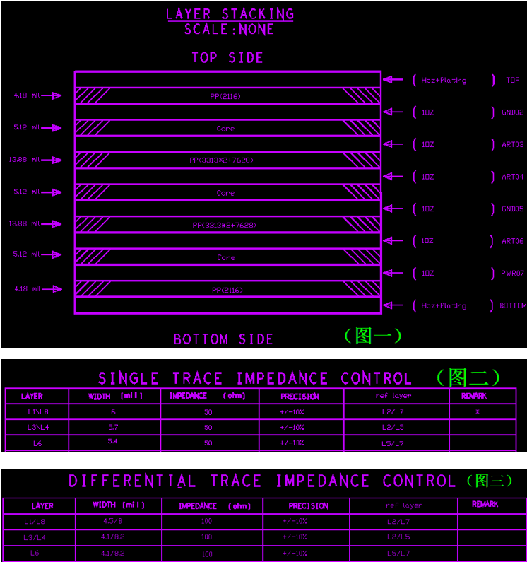
Signal lines that need to be impeded should be set strictly in accordance with the line width and line spacing calculated by the stack up . For example, for RF signals (conventional 50R control), important single-ended 50R, differential 90R, differential 100R and other signal lines, the specific line width and line spacing can be calculated by the layer stacking, as shown below.
The production process capabilities of the selected PCB production plants should be considered when designing the line width and line spacing, if the design of the line width line spacing set to exceed the process capabilities of the cooperative PCB manufacturers, it at least need to add unnecessary production costs, and worst of all, will lead to the design can not be produced.
Normally, the line width and line spacing control to 6/6mil, with 12mil (0.3mm) via hole , basically more than 80% of PCB factories can produce, the lowest cost of production.
The minimum line width and line spacing is 4/4 mil, with 8 mil (0.2mm) via hole , basically more than 70% of PCB suppliers can produce, but the price is slightly more expensive than the first case, not too much.
The minimum line width and line spacing control to 3.5/3.5mil, with 8mil (0.2mm) via hole , some PCB fabricators can not produce, the price will be a little more expensive.
Line width and line spacing minimum control to 2/2mil, with 4mil (0.1mm , at this time is generally HDI blind buried hole design, need to use laser via hole) via hole , at this time , most PCB vendors can not produce, the price is the most expensive. Here the line width and line spacing set rules when referring to the size between elements such as line to hole, line to line, line to pad, line to via hole, hole to pad .
When setting up the rules you need to consider the design bottlenecks in the design files . If there is a n 1mm BGA chip , with shallow pin depth, only one signal line needs to go between the two lines of pins, it can be set to 6/6mil, and with deeper pin depth , 2 signal lines need to go between the two lines of pins, it can be set to 4/4mil . If there is a BGA chip with 0.65mm, it is generally set to 4/4mil; with 0.5mm, the minimum line width line spacing must generally be set to 3.5/3.5mil; with 0.4mm, HDI design is generally required. General for the design bottleneck, you can set the regional rules, local line width and line spacing set a small point, the rest of the PCB rules set some large, in order to produce, improve the production of PCB pass rate.
Need to be set according to the density of the PCB design, the density is smaller, the board is looser, you can set the line width and line spacing a little larger, and vice versa. Conventional can be set in the following steps.
8/8mil, over-hole selection 12mil (0.3mm)
6/6mil with 12mil (0.3mm) overholes
4/4mil with 8mil (0.2mm) over hole option
3.5/3.5mil with 8mil (0.2mm) over hole option
3.5/3.5 mil with 4 mil over hole option (0.1mm, laser punched)
2/2 mil with 4 mil over hole option (0.1mm, laser punched)