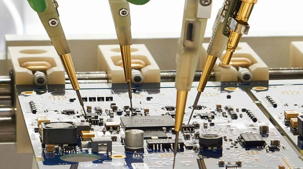
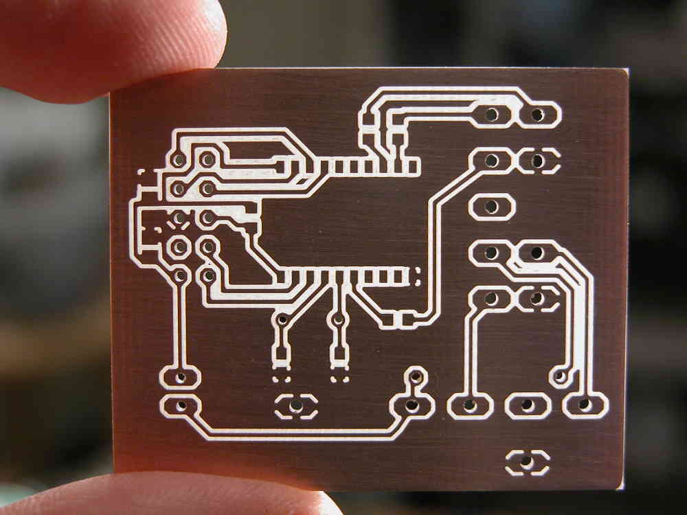
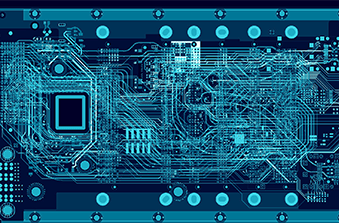
Technical Capabilities of Top-tier China PCB Enterprises(II)
Views: 1569Author: Site EditorPublish Time: 2023-05-26Origin: Site
SH Technology
SH Technology has the R&D and manufacturing capability of 70-layer high-precision PCBs and 20-layer fifth-order HDI PCBs. The company's high-density multilayer VGA (graphics card) PCBs and small-pitch LED PCBs have the world's largest market share.
CD Technology
During the reporting period of 2022, CD Technology completed the development of circuit board technology for Mini LED, circuit board signal integrity technology, high-precision impedance control technology, various surface treatment printed circuit boards, microphone packaging substrate based on the Cavity process, RF packaging substrate based on Tenting process, SiP packaging substrate based on ETS process, and refined circuit with high signal integrity. mSAP fabrication process and many other technology development work.
In the fourth quarter of 2022, CD Technology completed the world's first 28*49-inch large-panel production line and effectively solved the industry processes difficulties such as stability, uniformity, scrap rate, and operation complexity of large-panel mass production, and the large-panel process has now achieved mass production. Our subsidiary, Proware SiP packaging substrate (system level packaging) division, has further improved the integration of the company's packaging substrates by adopting mSAP, ETS, and ultra-micro via technologies to enhance the Trace Pitch to 30um, and the minimum finished board thickness has reached 0.11mm in mass production and has the capability of planar embedded capacitors, embedded resistors, chip embedding, and semi-embedding. process capability.
CS Electronics
In the printed circuit board business, the company has mastered the core technologies of high-frequency and high-speed printed circuit board technology, arbitrary layer interconnection printed circuit board technology, and automotive microwave radar printed circuit board technology, and has different printed circuit board production lines, which can accept orders across a large span of capacity covering HDI (including carrier-like boards), arbitrary layer interconnection, high-density multilayer boards, and fast board business, and has strong competitive strength.
XS Technology
XS Technology is recognized as a "National High-tech Enterprise", "National Intellectual Property Demonstration Enterprise" and "Innovative Enterprise of Guangdong Province", and has set up 3 provincial-level R&D institutions "Guangdong Provincial Enterprise Technology Center It has set up 3 provincial-level R&D institutions "Guangdong Provincial Enterprise Technology Center", "Guangdong Packaging Substrate Engineering Technology Research Center" and "Guangdong High-Density IC Packaging and Testing Substrate Enterprise Key Laboratory", and has the ability to undertake national-level government projects, and has undertaken 1 national science and technology major special project 02 and many provincial and municipal-level science and technology projects. In January 2022, Guangzhou Technology, a subsidiary of the Company, was selected as one of the pilot demonstration projects for Industrial Internet in 2021 by the Ministry of Industry and Information Technology of the People's Republic of China. In February 2022, Guangzhou Technology's "Load Board PCB for High-Speed Chip Test", "High-Performance Domestic High-Frequency Buried Resistance Mixed Voltage Tracking Radar Product" and "Thin ENEPIG (Ni thickness 0.5um) 5G RF Packaging Substrate" were selected by Guangdong High-Tech Enterprise Association as The three products were selected by Guangdong High-tech Enterprise Association as Guangdong Famous High-tech Products in 2021.
SY Electronics
SY Electronics has mastered large-size printed circuit manufacturing technology, three-dimensional structure PCB manufacturing technology, built-in capacitor technology, heat dissipation technology, graded gold finger manufacturing technology, micro-through-hole manufacturing technology, micro-blind-hole manufacturing technology (HDI), mixed pressing technology, micro-through-hole local insulation technology, N+N double-sided blind pressing technology, multilayer PCB graphic Z-alignment technology, high-speed signal loss control technology, high-speed high-frequency laminate process processing technology, 100G The company has maintained strong core competitiveness through core technologies such as 100G-400G high-speed optical module printed circuit board fabrication technology, and integrated PCB fabrication technology with built-in conductive medium and thermoelectricity.
OSK
(1) New product development: In recent year, OSK has focused on high-end server product development, and has introduced Eagle stream and Birch stream products into small batch production; successfully developed 77G radar, 5G antenna, double-sided amplifier buried copper and other technologies, and vigorously developed and innovated in 5 communication, high-speed server, storage, computer and other products, and has the process capability of mass production. New energy vehicles, increase market expansion and technology upgrades, from the traditional automotive consumer electronics gradually deep into the safety parts products; further strengthen the internal technical strength, has imported the inverter, charging pile, buried copper car products, car radar.MCU, VCM and other products, especially the development of semi-soft board production technology, mature in a number of car domain steering controller in batch application. At the same time, for further extension, from the traditional single-sided semi-soft board to double-sided semi-soft board, rigid-flexible combination board direction pre-research, the last two years will further broaden the product line, other cutting-edge special product development has also completed the technical reserves, layout of buried conductive adhesive, antenna I film products, cavity board, mechanical blind hole, step gold finger, high current tab board and a series of new varieties of development.
(2) Technical capability enhancement part: In terms of technology, we have developed new technologies such as skip via, 0.125mm super micro-hole, 0.8mm pitch BGA clip double line, D+6 back drilling, etc., especially for PCle 4.0 and DDR5 series communication products, to further extend the technology level (3) High-end material import research: In terms of high-end server and automotive safety parts, energy board product development In the development of high-end server and automotive safety parts and energy boards, we will further improve our material library, covering all material types from CEM-3, FR4, mid loss, low loss, very low loss, to Ultra Low-Loss, and expanding to high frequency PTFE materials, low orbiting satellite materials, special PI shielding film, P flexible materials, BT materials, etc. In automotive safety parts and energy boards, we will complete the introduction of safety parts material certification, and carry out high reliability and reliability research. In addition, we have conducted basic research on high reliability, high pressure resistance and high stability, and formed many original basic data to provide DFM design basis to ensure stable operation of highly reliable products. In particular, the testing of material pressure resistance, high reliability TCT, CAF, etc., from stack up design and material selection, process high reliability quality assurance products for long time stable application.
BM Electronics
After years of R&D and innovation, BM Electronics has developed a series of patented technologies with independent intellectual property rights. Among them, the representative ones are 1. "The method of burying capacitors in the printed circuit board and its printed circuit board", which is a passive component such as a capacitor or resistor placed inside the board, not only save space on the surface of the board but also reduces its weight and thickness. Reliability is also improved by eliminating soldering points. The embedding of passive components will shorten the length of the wires and allow for a more compact device layout, thus improving electrical performance, and has been selected as a pre-winning project for the China Patent Excellence Award (under public announcement) 2. Four years later, it was officially released. The release of this standard fills the gap in the industry in this field and provides technical support documents for the development trend of modularization and high integration of high-power devices in the communication market and "intelligent + new energy" vehicles. 3. The company has completed the development of PCB samples for the new generation of the EGS platform and has batch production capacity. Compared with the previous generation of platform products, EGS platform products in high-speed material application, processing density, and the number of design layers have been greatly improved.4, AMB ceramic village board technology has reached the international leading level, with independent intellectual property rights of brazing material technology, comprehensive mastery of the sintering, graphic etching to the surface treatment process, the product has superior performance, reliable quality, cost advantages, etc., mainly from The following indicators are measured:
(1) the cavity rate is controlled at 0.3%-0.5%;
(2) the cold and thermal shock (-55-175) can withstand more than 5,000 times;
(3) the cladding thickness is more than 0.8 mm, even up to 2 mm.