News
Site Editor
 Site
/uploads/image/667d0e0257f45.png
PCB, which stands for Printed Circuit Board, is an essential component in the world of modern electronics. PCBs serve as the foundation for the electrical connections and components that enable the functioning of various electronic devices. In this article, we will delve into the intricacies of PCBs and uncover their inner workings, exploring the fascinating world behind these seemingly ordinary circuit boards.
Unveiling the Inner Workings: Exploring the World of PCB
Views: 1718
Author: Site Editor
Publish Time: 2023-07-20
Origin: Site
Introduction:
PCB, which stands for Printed Circuit Board, is an essential component in the world of modern electronics. PCBs serve as the foundation for the electrical connections and components that enable the functioning of various electronic devices. In this article, we will delve into the intricacies of PCBs and uncover their inner workings, exploring the fascinating world behind these seemingly ordinary circuit boards.
 The Basics of PCB:
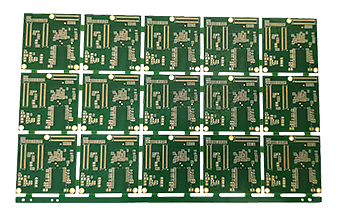
A PCB is a flat board made of non-conductive material, such as fiberglass, with conductive pathways etched onto its surface. These pathways, known as traces, are responsible for carrying electrical signals and forming connections between components. The traces are typically made of copper, which is adhered to the PCB through a process called etching. The copper areas that are not required for electrical connections are removed, leaving behind a network of interconnected traces.
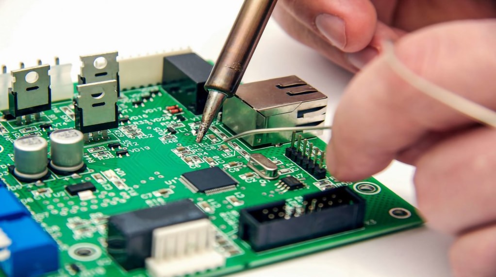
Components, such as resistors, capacitors, and transistors, are mounted onto the PCB using soldering techniques. These components are strategically placed and soldered onto the board, ensuring the efficient flow of electrical current and the proper functioning of the device. The design and layout of components and traces on a PCB are pivotal in determining the electrical performance of the device and minimizing potential interference.
The Manufacturing Process:
The manufacturing process of a PCB involves several crucial steps. It begins with the design phase, where the circuit board layout is created using specialized software. The design is then converted into a digital file, known as the Gerber file, which contains all the information required for production. This file is sent to the PCB manufacturer, who uses it for the fabrication of the board.
The fabrication process starts with the base material, usually a fiberglass epoxy laminate, which is cut according to the desired size and shape. The copper layers are then added to the board using a lamination process. After that, the excess copper is removed by etching, leaving behind the desired traces and patterns. The next step involves drilling holes for component placement and then electroplating them to create metal pathways within the holes.
Once the PCB is fabricated, it goes through an inspection and testing phase to ensure its quality and functionality. Automated optical inspection (AOI) and electrical testing are commonly used methods to identify any defects in the board. After passing the inspection, the PCB is ready to be populated with electronic components and undergo soldering to establish the necessary connections.
The Advancements and Future of PCB:
Over the years, PCB technology has made significant advancements, enabling the development of smaller, more efficient, and more complex electronic devices. Advancements such as multi-layer PCBs, surface mount technology (SMT), and flexible PCBs have revolutionized the electronics industry.
Multi-layer PCBs are designed with multiple layers of copper traces, separated by insulating material. This allows for more intricate designs and compact electronic devices. Surface mount technology, on the other hand, eliminates the need for drilled holes and uses smaller components that can be mounted directly onto the surface of the PCB, further reducing the size of electronic devices. Flexible PCBs, as the name suggests, are designed to be flexible and can be bent or twisted, making them ideal for applications that require flexibility.
The future of PCB technology seems promising, with ongoing research in areas such as printed electronics, 3D printing of PCBs, and the integration of more advanced materials. These developments aim to improve the performance, reduce the size, and enhance the functionality of electronic devices, further driving innovation in the industry.
Conclusion:
The world of
PCBs encompasses a myriad of technological wonders that contribute to the smooth functioning of our modern electronic devices. Understanding the basics, the manufacturing process, and the advancements in PCB technology provides insight into the intricate workings of these circuit boards and the constant evolution happening behind the scenes. As we continue to explore and innovate, PCBs will undoubtedly continue to be at the heart of our technological advancements, empowering a world of endless possibilities.
