Exposure
Exposure in Printed Circuit Board Manufacturing
In the process of manufacturing printed circuit boards, the exposure step plays a crucial role in transferring the circuit pattern onto a photosensitive coating. Let's delve into the details of this important stage:
Exposure is a key step in the production of PCBs, where the designed circuit pattern is transferred onto a photosensitive coating, typically using photolithography techniques. This step is typically carried out using a photolithography machine or exposure equipment.
To begin, a transparent mask is created, representing the desired circuit pattern. The mask consists of areas that correspond to specific sections of the copper or other layers on the PCB. The mask is then placed on top of the PCB, which is coated with a photosensitive layer such as a photo resist or photosensitive film.
Next, the mask and PCB are placed together in the exposure equipment. The equipment generates a specific light source, often ultraviolet (UV) light, to illuminate the pattern on the mask. The light passes through the transparent regions of the mask and reaches the photosensitive coating, while the blocked regions remain shielded.
During the exposure process, the light causes a chemical reaction within the photosensitive coating, known as the photo active compound. This reaction renders the exposed areas either soluble or insoluble, depending on the type of photosensitive material used. Following exposure, the remaining steps involve chemical treatment to remove or preserve the exposed regions of the photosensitive coating.
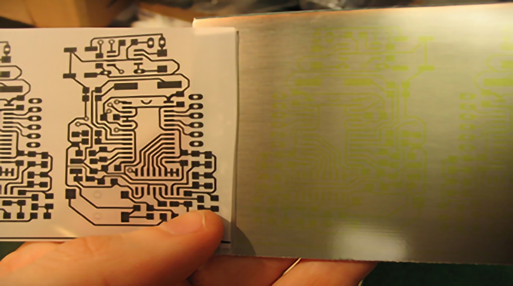
Upon completion of the exposure and chemical processing, the remaining photosensitive coating forms the desired pattern on the PCB. This pattern serves as a guide for subsequent processes such as etching, copper plating, soldering, or other fabrication steps to form the required circuit structures on the PCB.
In summary, the exposure step is a vital stage in the manufacturing process of printed circuit boards. It involves transferring the circuit pattern onto a photosensitive coating, providing an accurate guide for subsequent processing steps.
The precise execution of the exposure step ensures the successful reproduction of the circuit pattern, enabling the creation of functional and reliable electronic circuits. Through careful control and optimization of the exposure parameters, manufacturers can achieve high-quality PCBs that meet the stringent requirements of modern electronic devices.
In conclusion, the exposure step is a critical stage in the production of printed circuit boards, contributing to the accurate replication of circuit patterns. It forms an integral part of the photolithography process, paving the way for the fabrication of intricate and precise circuitry on PCBs.