Technology
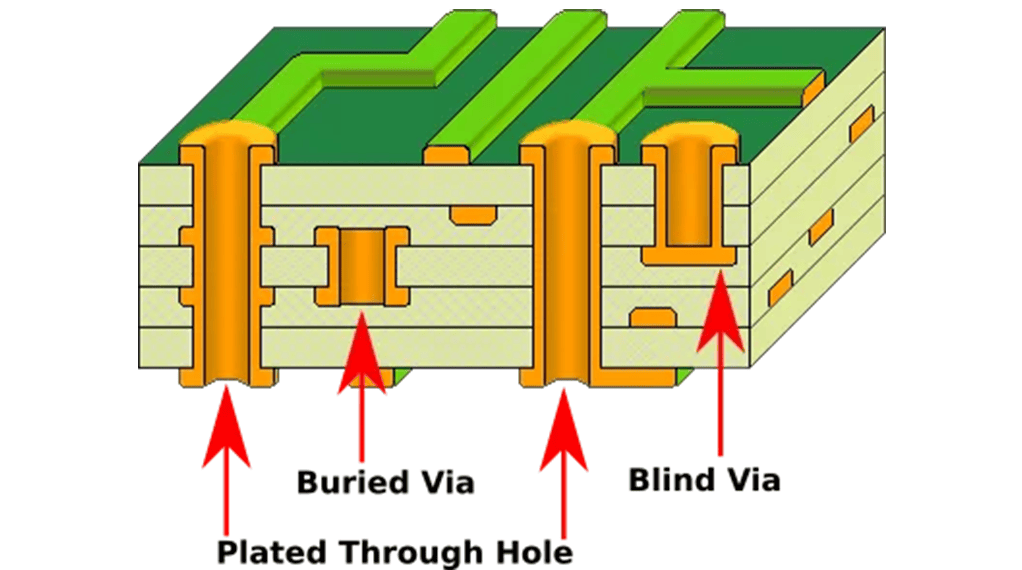
PTH
Copper Plating in Printed Circuit Board Manufacturing
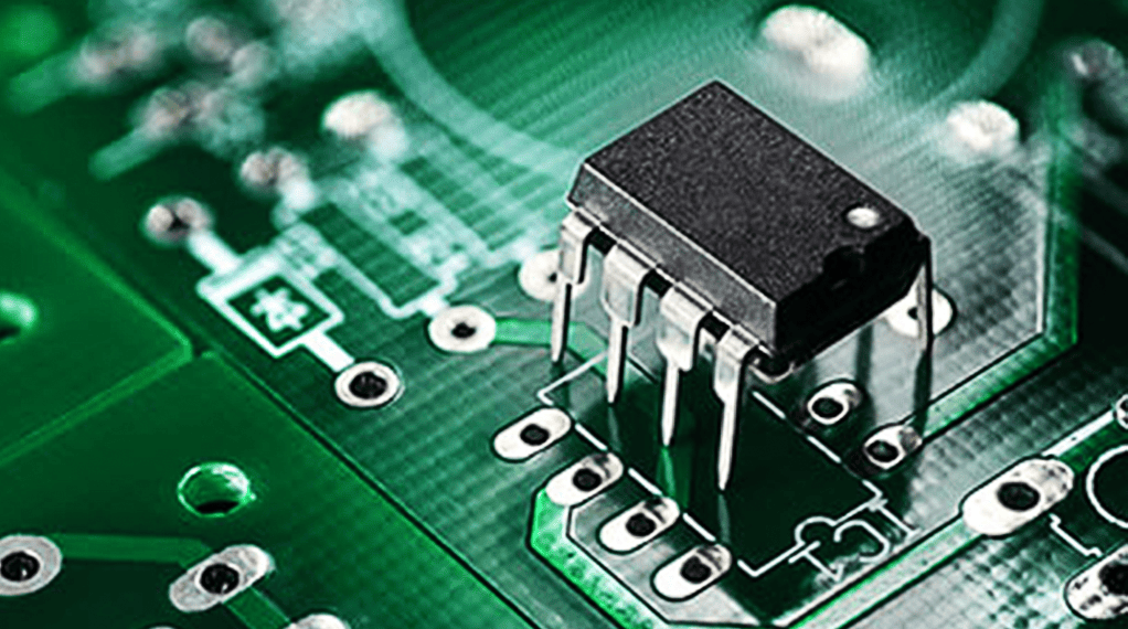
Printed Circuit Boards are crucial components used in a wide range of electronic devices, including smartphones, computers, and industrial machinery. These boards serve as the backbone for electrical connections and components within electronic circuits. An integral step in PCB manufacturing is copper plating, also referred to as copper deposition.
Copper plating involves electrochemically depositing a layer of copper onto the surface of the PCB. This process is employed to create a conductive layer that enables the flow of electrical current and imparts structural integrity to the board. Copper plating typically follows the preparation of the substrate and the creation of the circuit pattern.

The copper plating process commences with thorough cleaning and activation of the PCB surface. The board undergoes a meticulous cleaning procedure to eliminate any impurities, such as dust, grease, or oxidation, that might hinder the adhesion of the copper layer. Once the surface is clean, it is activated using an etching solution or a chemical treatment to enhance adhesion and promote effective bonding between the copper and the substrate.
After the cleaning and activation steps, the PCB is immersed in a copper plating bath containing a copper sulfate electrolyte solution. The bath comprises copper ions that will be deposited onto the PCB surface. The PCB is connected to the cathode, while a sacrificial copper anode is connected to the anode. When an electric current is applied, copper ions from the anode dissolve into the electrolyte, migrate to the cathode, and deposit as a thin layer of copper.
The deposition rate and thickness of the copper layer can be controlled by adjusting parameters such as current density, plating time, temperature, and copper concentration in the bath. Careful monitoring and control of these parameters ensure uniform and precise copper plating across the entire PCB surface.
Once the desired copper thickness is achieved, the PCB is removed from the plating bath and thoroughly rinsed to eliminate any residual electrolyte or by-products of the plating process. The copper layer is then inspected for uniformity, adhesion, and quality. Additional steps, such as surface finishing or solder mask application, may be performed subsequently to safeguard the copper layer and facilitate further assembly processes.

Copper plating plays a critical role in PCB manufacturing by providing a conductive layer that enables the smooth flow of electrical current and supports the interconnection of electronic components. Additionally, it enhances the structural integrity of the PCB, rendering it more robust and durable. The quality of the copper plating directly impacts the performance and reliability of the final electronic device.
In conclusion, copper plating is an essential stage in the production of printed circuit boards. It involves electrochemically depositing a copper layer onto the PCB surface, which imparts conductivity and structural support. By carefully controlling plating parameters and conducting thorough inspections, manufacturers can ensure high-quality copper plating, resulting in reliable and efficient electronic devices.


